"SHUT UP Device" - Part 2
Now it's time to display thingsWelcome back! In the second part of this series, I'm adding something extra to the project and adding a small monochrome OLED display to the project. While the display content is going to be simple, it gets complicated because I have to implement a driver for this from scratch in Rust (with some existing C reference code).
The time to talk has passed. The lord's work must be done. (Joshua Graham, Fallout: New Vegas).
Shifting Pixels
Whenever a peripheral is added to a hardware project, it is important to understand how to operate it and interface it with the rest of the project; On the software side, it's a similar notion to adding a library to a project. In this case, the processor of the project would be interacting with a display controller connected to a black-and-white OLED screen with the size of 128 pixels (px) by 64px. Think of it as a very miniature graphics card. I don't plan on going into the specifics of how such a controller is designed since that isn't fully needed to write a minimal driver, but this video by Ben Eater on how to make a VGA display controller on the hardware level is an excellent watch and has some transferrable concepts.
Heads up, this section abstracts the underlying method of communication (a.k.a. the "protocol") since the display controller in question (the SSD1306) supports multiple methods of communicating with a processor or other circuit. The section after this will talk about the method I chose for communicating with the controller, but otherwise this section is written under the assumption that any valid protocol is used. You can always refer to the datasheet of the display controller for more information.
A Really Specific Processor
For this project, I used a SSD1306 128x64 monochrome OLED display. This is a fairly well established part and has variants depending on the size of the display or other needs. While the full circuit is very complicated due to the amount of data lines the chip uses, the block diagram provided by the datasheet elucidates quite a bit about the design:
](/blog/0008/oHjI1ufgeO-812.webp)
What I gathered from this diagram (based on background knowledge and more of the datasheet) is that this is a very simplified CPU. Sure, there might not be an ALU or a register file, but the reason I consider it as such is that it takes inputs that could be interpreted as machine code. This acts more like G-Code from the machinist and CAM world but instead of moving motors or extruders "commands" manipulate the physical pixels, which are stored in the Graphics RAM.
Continuing the comparison to machine code, the datasheet has an entire section about what signals and bits need to be set for different actions such as changing oscillator speeds or setting pixels. One of the most important signals is the "Data/Command (D/C)" bit which controls the interpretation of whatever is being sent over the data bus (indicated with pins D0-D7); if the signal is high, data from the bus is written to RAM, otherwise (when low) it is pushed to the command decoder and changes internal display state wizardry. When paired with the "Read/Write (R/W)" signal, it allows for controlling the direction of data on the bus and what the source of the data is (see Table 9-3 in the datasheet). This project only writes to the display, so the R/W signal is always set to have the bus write to the display controller.
](/blog/0008/PgO9BgRJuw-812.webp)
There are a good chunk of commands, but most of these are only relevant when initializing the display on power up, such as changing how the RAM is mapped to the physical pixels (via the internal drivers). Depending on how processor code is written, an "initialization command list" can be created to ensure a consistent live configuration of the display is preserved whenever the device is powered on. Having this also allows enforcement of certain semantics when writing to the display (more on that in a bit), which ensures a consistent internal state on initialization.
/// Set Lower Column Start Address for Page Addressing Mode.
const SSD1306_SETLOWCOLUMN: u8 = 0x00;
/// Set Higher Column Start Address for Page Addressing Mode.
const SSD1306_SETHIGHCOLUMN: u8 = 0x10;
/// Set Memory Addressing Mode.
const SSD1306_MEMORYMODE: u8 = 0x20;
/// Set display RAM display start line register from 0 - 63.
const SSD1306_SETSTARTLINE: u8 = 0x40;
/// Set Display Contrast to one of 256 steps.
const SSD1306_SETCONTRAST: u8 = 0x81;
/// Enable or disable charge pump.  Follow with 0X14 enable, 0X10 disable.
const SSD1306_CHARGEPUMP: u8 = 0x8D;
/// Set Segment Re-map between data column and the segment driver.
const SSD1306_SEGREMAP: u8 = 0xA0;
/// Resume display from GRAM content.
const SSD1306_DISPLAYALLON_RESUME: u8 = 0xA4;
//...
With the information to initialize the display, it is now time to change some pixels and write some letters.
Addressing Semantics and Character Maps
When looking at the data bus, it is only 8 bits wide. Yet there are 8192 pixels on the display that can be switched on and off. Obviously, it is not efficient to try and connect all 8192 pixels directly to a microcontroller, that is why the display controller exists. But how does the display controller know where to turn on the pixels? Short answer, it's based on whatever is in the Graphics RAM (from the block diagram). But a more correct (and necessary) answer is required to even consider displaying anything meaningful. Section 8-7 of the SSD1306 datasheet is very revealing about how the graphics RAM represents the pixels on the screen. While in reality the RAM is effectively a contiguous block, the block is abstracted into 8 "pages", each representing a 128x8 portion of the display. There are no specific details how these pages are implemented, but it could be a very simple implementation involving a multiplexer (mux) that selects a RAM block to manipulate (this is speculation).
](/blog/0008/Aj_VB_bVhj-708.webp)
Even when working in the smaller address space under the pages, that is still 1024 pixels that need to be managed and can't really be connected en-masse to the microcontroller. Plus, a page in this case is a smaller contiguous block of RAM which can be mapped to the physical pixels in different ways. It's not dissimilar to how a multidimensional array can be represented in different ways while maintaining a flat-array footprint in C:
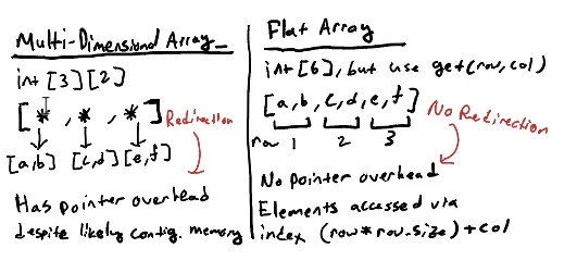
Again, all of this functionality is abstracted by the display controller, what matters is what possible address mappings are available. In this case the three modes are page addressing, horizontal addressing, and vertical addressing. Depending on what is being drawn, a different addressing mode would allow for more efficient interaction by requiring less data commands sent to the display peripheral. For example, Drawing a horizontal line is effectively more efficient using horizontal addressing than vertical addressing; Under vertical addressing, the same byte sequence would need to be drawn 8 times instead of a single sequence horizontally. However, drawing complicated shapes like letters make more sense when using vertical addressing since it would be more "information dense" (i.e. it uses fewer bytes to represent the same information). Given that vertical addressing sticks within the boundaries of a page, it means that each byte written represents a vertical "slice" of a character and there is no need to send any "cursor change" commands.
To efficiently display characters without doing too much math, a constant table containing the respective byte sequences for each character is added to the project. In a sense, this is creating a simple bitmap font which can easily be indexed against ASCII Codes; by default strings are already stored in an encoding that extends ASCII so minimal effort is needed to perform the mapping. Each character is sized at 5x7 pixels, which means the last row of each character can be reserved as a built-in space and align with the row count of memory pages. To save space on the limited memory, unused symbols and the control codes can be removed and a little bit of math can still provide a one-to-one mapping for alphanumeric characters:
//Assumes 0 = ASCII 0x20 or ASCII 32
const FONT_DATA: [[u8; 6]; 96] = [
    [0x00, 0x00, 0x00, 0x00, 0x00, 0x00], // (space)
    [0x00, 0x00, 0x5F, 0x00, 0x00, 0x00], // !
    [0x00, 0x07, 0x00, 0x07, 0x00, 0x00], // "
    [0x14, 0x7F, 0x14, 0x7F, 0x14, 0x00], // #
    [0x24, 0x2A, 0x7F, 0x2A, 0x12, 0x00], // $
    [0x23, 0x13, 0x08, 0x64, 0x62, 0x00], // %
	//...
]
The only remaining "gotcha" is the notion of the "cursor", or the point in memory where sent data is (over)written in the graphics RAM. While the exact implementation may be black-boxed, using the command details from the datasheet indicates it's stored as a 3-byte "address": 1st byte being the memory page, and the 2nd and 3rd byte pointing to the row and column of that page. The most likely reason for such an addressing scheme (speculation) is to allow for displays with different sizes to have a similar interface and thus allowing easy interoperability on a hardware level, even though smaller displays have larger regions of "address space" that are unused. An important note is that the actual position of the cursor can be accessed but would require adding extra communication and worrying about bidirectional signaling (which I²C does have) given it requires a read operation. A reasonable alternative is to also track the cursor state in the microcontroller and manipulate it as data is written to the display controller. When initializing the display controller, A cursor set command can be used to put the cursor at the origin, and extra code during write operations using the known sizes of each bitmap character allows maintaining accurate knowledge of the display controller's state without having to read it at all. This method might not work for more complicated display controllers, but it works for the very rudimentary driver being created.
//Very smol
pub struct SSD1306Display {
    col: u8,
    row: u8,
}
The cool thing about a custom driver is not all features of the client device have to be used. While modern compilers often optimize and remove unused code, not having to worry about such code in the first place allows for projects to be less complex and easier to work on. When writing the driver, I used the SSD1306 ASCII library for Arduino as a solid reference, but it had features related to the scrolling functionality of the display, using other font types, and broader display interoperability (remember the addressing discussion?). Cutting down the fluff and only implementing what was needed means the driver was actually written faster than if I chose to do a full library port. It might be a fun exercise, but it isn't the focus of the project at all.
With all the information about how the display (controller) works, it is now time to actually have the microcontroller "talk" with the controller. While the display peripheral comes in different protocol variants, I chose the I²C variant for simple wiring. But that simple wiring comes at the cost of protocol complexity.
The I-squared-C protocol
Inter-Inter Circuit Communication (shortened to I2C and stylized as I²C) is a specification for bidirectional signaling between multiple complex integrated circuits over two wires: "Serial Data (SDA)" and a "Serial Clock Signal (SCL)". Also documented as the Two-Wire (Serial) Interface or TWI in microcontrollers like the ATMEGA328P used in the project, it was developed by Phillips Semiconductors (now owned by NXP) as a way to communicate between many processors, microcontrollers, and the like. As a standard, it boasts an impressive amount of flexibility in configuration, supporting up to 127 uniquely addressed devices and multiple controllers on the same bus. I wouldn't be surprised if a computer uses them for different peripherals.
Given it has been a while since I touched I²C communications (because I haven't done embedded for a couple of years), I decided to do the most reasonable thing and read the official specification of the standard, which is provided by NXP for free online. While it contains a boat load of information that isn't fully relevant to this project such as multi-controller arbitration or ultra-fast mode (a very cool name :P), the core information about how communication between controllers and targets is there.
For this overview, I plan on skipping over details like electrical specifications and fault handling while making the examples related to communicating with the display controller. This is not to say generic implementations and details aren't important, and when doing something like designing a multipurpose microcontroller this information is absolutely necessary!
"Instant" Messaging over Wires
The I²C protocol is based on "transactions" initiated from a controller to an addressed target (in older documentation, the terms "master"/"slave" are used instead, but due to obvious connotations the new naming is preferred in modern day). The addressing is important as multiple devices could be connected to the bus, so designating which target peripheral should activate within a transaction is crucial to ensuring the right action is performed. For those who do modern backend programming, I find it similar in concept to a "targeted" UDP for lack of a better description given the notion of sending data to multiple clients, the core difference is that a single client usually responds to a message (if such an addressed client exists). Each transaction begins when the controller sends a start condition and (ends) successfully when the controller sends the stop condition, which is based off of the specific state of SDA and SCL over a certain period of time.
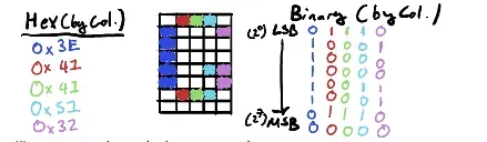
](/blog/0008/Ztcmy4z4YE-541.webp)
Within each transaction, messages are sent in 1 byte (8 bits) "packets", with each packet being followed by an acknowledge bit before the next byte is sent. This acknowledge works similarly to how a start/stop condition is detected, making it clear when a target (or the controller if it is reading from a target) is ready for the next byte.
](/blog/0008/3F4t7ioGfJ-680.webp)
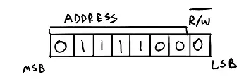
At the beginning of each transaction, the first byte sent over the bus is the 7-bit address of the target peripheral to communicate with plus a read-write (R/W) bit indicating the direction information is sent on the bus (read means target to controller, write is the opposite). While reading from a device is the only way to interact with certain peripherals, the plan is to only write to the display controller, so all future examples will assume a controller-target communication scheme and thus the R/W bit will be 0 due to it being active low. Given the I²C address of the controller being 0x3C, the first byte of each transaction would actually be 0x78 since the 7-bit address uses the most significant bits (MSB) of said byte.
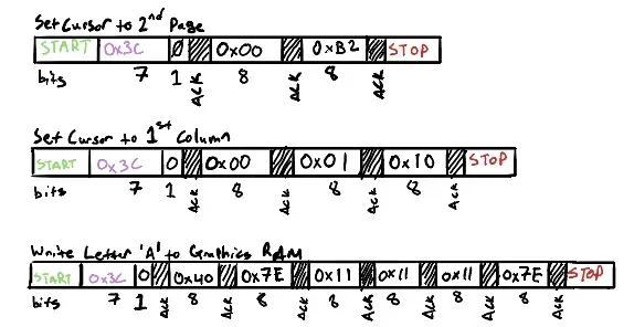
After the transaction is established and the first message is acknowledged by the controller, a control byte is sent by the controller, followed by a number of data bytes (not documented but up to 16 based on code I've tested). The control byte is basically empty but is otherwise important since because the 7th MSB serves as the D/C signal mentioned earlier. However, this makes the code a lot easier by knowing that 0x00 will have the following bytes be treated as commands, whereas 0x40 indicates the following bytes are for writing to the graphics memory. Putting it all together, these are the example transactions to display a capital 'A' on the second line:
Writing it in code
What if I said that there was no need to learn half of this information. Well it's kinda true. Many hardware abstraction layers (HALs) for devices that support I²C usually create a simplified software interface to perform I²C operations on the controller side; The Arduino Core Library in C and the avr-hal crate used in the project abstract all of the I²C signaling specifics to the transaction level as discussed previously. Obviously, mileage will vary depending on the project, but any good programmer can wrangle bytes to make things work in places they shouldn't. Like running DOOM on everything in existence. Although admittedly that is a bit cooler than this.
The first thing to acknowledge is the initialization of the I²C abstraction in code. For the avr-hal crate, it looks roughly like this:
let mut i2c = arduino_hal::I2c::new(
	dp.TWI,
	pins.a4.into_pull_up_input(),
	pins.a5.into_pull_up_input(),
	400000,
);
I won't go into too much depth here about what this does under the hood, but I want to point out a couple of interesting factoids:
- The 400k value defines the bit rate of the I²C bus (or effectively the frequency of SCL). Something I glossed over previously, but some I²C implementations can support up to 10 MBits/sec, a.k.a. "ultra-fast mode" (very cool name). Either way, this is "fast mode" and is 4x faster than the basic 100Kbit/sec "normal mode." See section 3.1.1 of the spec.
- Despite being a digital bus, analog pins are used as SDA/SCL. This is part of the electrical specification details that I skipped, but "logic high" and "logic low" signals are based off of a percentage of a reference voltage; More specifically, logic high is minimum 70% of the reference voltage, logic low is maximum 30% of said voltage, the remaining zone is effectively "floating" or undefined. See section 3.1.2 of the spec.
The actual struct representing the display in the code is "light" in stored data: just the position of the "cursor" as mentioned earlier. Most of the functionality is with the associated methods with the struct, which always take a mutable borrowed I2c instance as a parameter. This has to do with lifetime checking and ownership rules that make Rust as a language "safe" (with some asterisks); By limiting access to memory and checking the validity of memory reads and writes, it allows elimination of entire bug classes such as use-after-frees, buffer overflows, and more. As a result, certain "C-like" paradigms such as global variables/memory regions which are useful in embedded contexts given they can help encode microcontroller register/bus state in a shareable manner are much harder to use since such access is inherently "unsafe". This will be discussed a lot more in the last part of this series, but some tidbits are important to acknowledge now to help with understanding the design decisions made.
Before anything can be written on the display, the display configuration needs to be completed to ensure a synchronized state. This is conveniently done in the new() function:
impl SSD1306Display {
    pub fn new(wire: &mut arduino_hal::I2c) -> Result<Self, Error> {
        #[rustfmt::skip]
        let mut display_init_seq: [Operation;26] = [
            Write(&[0x00]),
            Write(&[SSD1306_DISPLAYOFF]),
            Write(&[SSD1306_SETMULTIPLEX]), Write(&[0x3F]),         // ratio 64
            Write(&[SSD1306_SETDISPLAYCLOCKDIV]), Write(&[0x80]),   // the suggested ratio 0x80
            Write(&[SSD1306_SETDISPLAYOFFSET]), Write(&[0x0]),      // no offset
            Write(&[SSD1306_SETSTARTLINE]),                         // line #0
            Write(&[SSD1306_CHARGEPUMP]), Write(&[0x14]),           // internal vcc
            Write(&[SSD1306_MEMORYMODE]), Write(&[0x02]),           // page mode
            Write(&[SSD1306_SEGREMAP | 0x1]),                       // column 127 mapped to SEG0
            Write(&[SSD1306_COMSCANDEC]),                           // column scan direction reversed
            Write(&[SSD1306_SETCOMPINS]), Write(&[0x12]),           // alt COMWrite(&[pins]), disable remap
            Write(&[SSD1306_SETCONTRAST]), Write(&[0x7F]),          // contrast level 127
            Write(&[SSD1306_SETPRECHARGE]), Write(&[0xF1]),         // pre-charge period (1, 15)
            Write(&[SSD1306_SETVCOMDETECT]), Write(&[0x40]),        // vcomh regulator level
            Write(&[SSD1306_DISPLAYALLON_RESUME]),
            Write(&[SSD1306_NORMALDISPLAY]),
            Write(&[SSD1306_DISPLAYON]),
        ];
        match wire.transaction(I2C_ADDR, &mut display_init_seq) {
            Ok(_) => Ok(Self { col: 0, row: 0 }),
            Err(err) => Err(err),
        }
    }
}
It's a very simple function: send the entire initialization sequence, if it fails just stop doing anything since the device is in a failure state. This is another important notion that will be discussed in part 3, but from a more surface-level reasoning it is often better for a malfunctioning machine to stop operating than to keep trying to run and output flawed information. This function also returns the struct that can be used to interact with the display.
There are not many operations required to operate the display for this project specifically: write characters, write many characters, change the cursor position, and clear the screen (more a convenience method). Each operation is done in its own I²C transaction, which results in a similar structure for all those methods; Perform an I²C transaction with a specific byte sequence, then update internal state if needed. Robust error handling for I²C errors were ignored since it's a hobby project that is easily reset-able. Writing characters on the display is simple, but could be more efficient in theory with a "streaming" type operation whereas characters are read from the string the display is update. As the characters in the string are iterated through, the ASCII value is checked and then the respective bitmap sequence from the font table is retrieved and sent as an I²C transaction. Sure, it seems like too many transactions are being started and stopped but the overhead of the I²C protocol is not too important for this project; The notion of streaming the bitmaps would be nicer but requires added complexity to the project (I digress). Since strings are just arrays of characters, adding support for String or &str is as simple as calling the write() function on each character.
//impl SSD1306Display
pub fn write(&mut self, wire: &mut arduino_hal::I2c, ch: char) -> usize {
	match ch {
		'\r' => {
			//Carriage return only sets cursor to beginning of row similar to typewriter (hence why ms-dos uses \r\n)
			self.col = 0;
			1
		}
		'\n' => {
			self.set_cursor(wire, 0, self.row + 1).unwrap();    //TODO this is an easy crash we should handle but lazy :p
			1
		}
		' ' => {
			//Handle as a "non-font" space (i.e. not 5px long)
			//I'm choosing two as a nice choice
			self.write_ram_buf(wire, &[0x00, 0x00]);
			self.col += 2;
			1
		}
		ch if (ch as u8) > 0x20 && (ch as u8) < 0x80 => {
			let ascii = ch as u8 - 0x20; //Space is covered in prev branch
			let byte_seq = FONT_DATA[ascii as usize];
			//In theory, this should just work as is given we have no significant modification
			self.write_ram_buf(wire, &byte_seq);
			self.col += 6; //Add a little buffer space
			1
		}
		_ => 0, //Just ignore the character
	}
}

pub fn write_str(&mut self, wire: &mut arduino_hal::I2c, str: &str) -> usize {
	let mut count = 0;
	for ch in str.chars() {
		count += self.write(wire, ch);
	}
	count
}

fn write_ram_buf(&mut self, wire: &mut arduino_hal::I2c, bytes: &[u8]) {
	//This is "optimized" since the buffer mode allows for 16 bytes to be processed in a single command
	bytes.chunks(16).for_each(|chunk| {
		match wire.transaction(
			I2C_ADDR,
			&mut [Operation::Write(&[0x40]), Operation::Write(chunk)],
		) {
			Ok(_) => (),
			Err(_) => (), //TODO Better err handling!!!
		}
	});
}
And (after skipping a bunch of nuances that I want to avoid digging into) voilà! There is now a working display driver in the project.
Post-Credits Scene
Again, this post was delayed and pushed for many reasons. Aside from double-checking datasheets and industry specifications (which I really didn't have to do), many things happened in my personal life such as starting (more like continuing) a new job or getting somewhat addicted to the Elder Scrolls Oblivion Remaster. I still enjoy writing these posts and all the research and drafting that goes into it; The reMarkable tablet has helped greatly with speeding up the drafting process by being a quiet slate to write.
The next post is currently slated to be the last in this series, where I discuss embedded programming, primarily focusing on some of the interesting "discoveries" I made while working with embedded Rust. At that point, I plan on making the repository for the project public, and will update all the posts in the series to reference it. No firm ETA on that, my Oblivion save RPing as the Green Goblin awaits, See you in the next one!